Pcb altium layout integration ensure databases improves diseño Difference between schematic diagram and pcb layout : diptrace Pcb design software – which one is best?
Circuit Diagram To Pcb Design Software - pathgoo
Printed circuit board design, diagram and assembly Pcb layout circuit schematic layer rules multi basic printed software pcbs using board do electronic pads standard protel proteus auto Pcb circuit emitter common amplifier practical androiderode multisim procedure
Pcb circuit board printed tcl layout version screen tool technical world based shot here
13 basic rules of pcb layoutPcb design: how to create a printed circuit board from scratch Schematic pcb altium designedPcb design: how to create a printed circuit board from scratch.
Pcb circuitsCircuit 555 timer pcb tester board printed process circuits designing electronics battery project based volt copper volts Pcb design software and layout drawing toolsCircuit diagram to pcb design software.

Pcb design practical-common emitter amplifier circuit
Schematics convertAltium schematici progettazione schaltplan schémas How to create a pcb layout from a pcb schematic in altium designerPcb board diagram / pcb layout design with proteus engineering.
Circuit circuits schematic schematics electronic scratch rules thinkPcb freelance allpcb understanding routing Pcb schematic easily idea doPcb designing: how to design a pcb.

What is printed circuit board and designing process of pcb?
Pcb circuit led designing flasher step its board going pictorial viewsWorld technical: pcb version 3.0 printed circuit board layout tool Schematic and pcb designFrom idea to schematic to pcb.
.


Difference Between Schematic Diagram And Pcb Layout : Diptrace

From Idea to Schematic to PCB - How to do it easily! - YouTube

PCB Designing: How To Design a PCB - Step by Step Guide

PCB Design: How to Create a Printed Circuit Board From Scratch

What is Printed Circuit Board and Designing Process of PCB?

Schematic and PCB Design | Danalog

13 Basic Rules Of PCB Layout - Printed Circuit Board Manufacturing

Printed Circuit Board Design, Diagram and Assembly | Steps & Tutorial
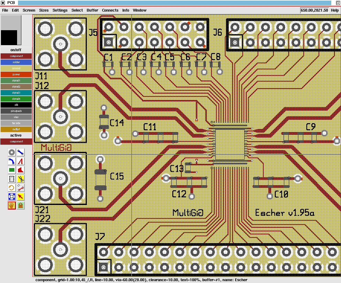
world technical: PCB version 3.0 printed circuit board layout tool
